Using Boundary Scan for PCB debugging
I did a seminar talk on JTAG and how to use it to check a PCB for errors. For this i designed a little board in order to simulate manufacturing errors. In this post I want to give you a short introduction to JTAG and how to use it.
What is Boundary-scan
Boundary-scan was developed to simplify testing of integrated circuits. To do this the Joint Test Action Group introduced the Boundary Scan architecture as a standard and today it has replaced the old testing methods because of its cost efficiency and speed up of test development and execution.
So how does this work?
I will be just covering the basics here. If you want a more detailed introduction, you can read the articles referenced at the end of this post.
Boundary-scan is a technology which places cells at the circuits boundary that can sample the circuit inputs and also drive its outputs. This can be done while the circuit is operating and it is controlled via the JTAG interface. With these cells in place we wan test the internal logic of the circuit as well as the interconnects between the devices on a board.
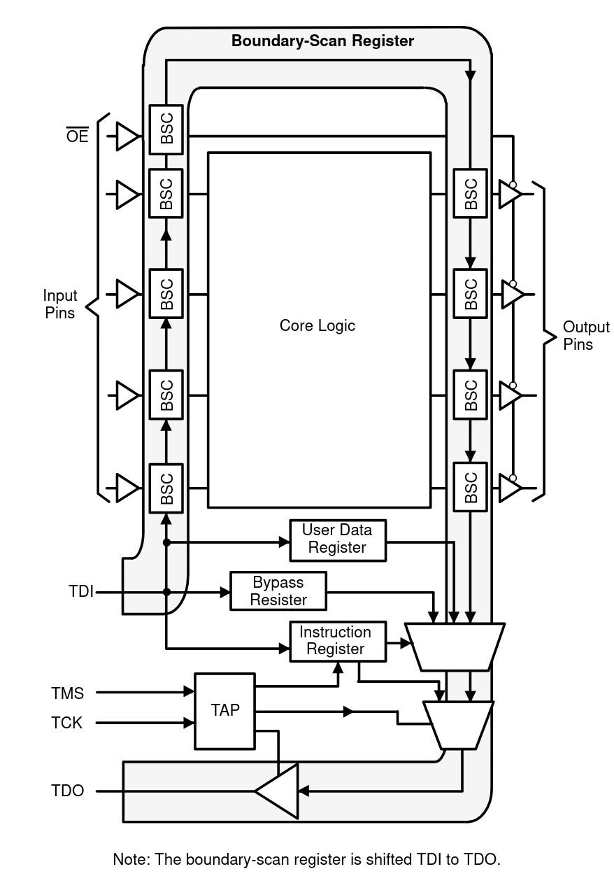
In the picture above you can see an overview of the boundary-scan architecture. This picture only shows one JTAG device, but on more complex PCB there are many such devices that are connected in a JTAG chain. This means that the data out of one chip is connected to the input of the next.
In order for us use this architecture, we need to connect to the four JTAG pins:
- TDI Test Data In
- TDO Test Data Out
- TCK Test Clock
- TMS Test Mode Select
Once connected we can control all of the devices in the JTAG chain. In general we can perform two different types of actions. We can either write/read data or we can write instructions. Testing a circuit involves both of theses actions. By writing instructions we can set the connected circuits into different modes. And by writing data we can set the pins to the desired levels as well as read the results.
There are three different instructions we are interested in when testing interconnects:
- SAMPLE/PRELOAD
- EXTEST
- BYPASS
With the SAMPLE/PRELOAD instruction the boundary-scan cells will sample the inputs of the circuit, and when shifting in data we can read values received at the pins. We can also use this command to load data into the boundary-scan cells. The EXTEST instruction will set the output of the pins to the values provided in the boundary-scan cells and the BYPASS instruction lets us skip devices in the chain that are not of interest to the test currently performed.
With these instructions we can set pins of a device to a logic level and test at the receiving circuit if the correct logic level was received.
The Hardware
We need to connect to the JTAG pins of a devices. If they are exposed there probably is a connector on the board. If not it may be possible to solder wires directly to the pins. In any case we will need a JTAG adapter in order to connect them to a normal computer via USB. I am using a JLink adapter which features a 20 pin JTAG connector.
The PCB I am using for testing is a small circuit I designed myself, it also has a 20 pin connector which exposes the JTAG pins. Here is the layout:
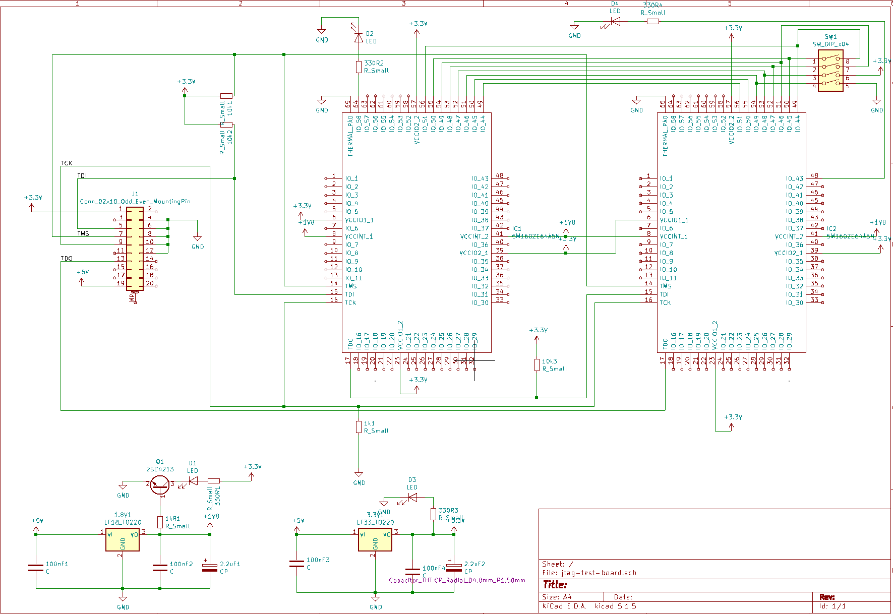
It features two MAX V Altera CPLDs that implement the boundary-scan architecture and are connected in a JTAG chain. To test some connections between them I connected eight of their pins at the top and added a dip switch to simulate shorts between the wires as well as pull ups and pull downs.
Tooling
Okay so we got a PCB and connected it to a computer with a JTAG adapter now what? How do get the tests running?
Well this is where it gets hard, because there is no nice open source software that does it all for us. We need to write the test ourselves and for that we need to know the details of the interconnects on our PCB and the details of how the boundary-scan architecture is implemented in the devices in our JTAG chain.
BSDL Files
The Boundary-scan standard does not tell manufacturers what bit codes to use to encode the instructions, but it does require them to publish the so called BSDL (Boundary Scan Description Language) files free of charge for their devices. These files use a dialect derived from VHDL a hardware description language and describe all information needed to use a devices boundary-scan architecture. For example:
- Instruction register description
- Boundary-scan cell description
- Pin mappings
- and more
Basically all information we might want to know about a specific device is in that file.
SVF Files
Most JTAG adapter tool chains support a file format called SVF (Serial Vector Format). These are plain text files that describe what data or instructions to write to the JTAG connection. It has no knowledge about the JTAG chain of devices or any of there properties. We can just specify what data/instructions to shift in and what results we expect to be shifted out.
Designing a simple test
Okay so putting it all together. Lets say we want to test two neighboring interconnects for a bridging fault.
On my example PCB two neighboring interconnects are connected as follows:
- CHIP 1 IO56 - CHIP 2 IO49
- CHIP 1 IO55 - CHIP 2 IO50
So if we set IO56 of the first chip to a logic 1 and IO55 to logic 0, we would expect to receive a logic 1 on IO49 and a logic 0 at IO50 on the second chip. If we receive a logic 1 at IO50 that means that there is a bridging fault between the interconnects.
To write a test for this we need to write an SVF file that we can run with the JTAG adapter tool chain. It needs to complete the following steps:
- Set first chip into SAMPLE/PRELOAD mode. (Shift in Instructions)
- Load Test pattern into first chip (Shift in Data)
- Set first chip to EXTEST and second chip to SAMPLE/PRELOAD mode (Shift in Instructions)
- Shift in dummy data to receive the data sampled from chip 2 and compare against the expected result (Shift in Data)
The following SVF files does exactly this:
TRST OFF;
ENDIR IDLE;
ENDDR IDLE;
STATE RESET;
STATE IDLE;
FREQUENCY 10000000 HZ;
SIR 20 TDI (01405);
SDR 480 TDI (000000000000000000000000000000000000000000800000000000000
	000000000000000000000000000000000000000000000000000000000000000);
SIR 20 TDI (03c05);
SDR 480 TDI (0) TDO (000000000000000000000000000000000000000000000000
	00000000000000000000000000000000000000000000000100000000000000000
	0000000) MASK (00000000000000000000000000000000000000000000000000
	00000000000000000000000000000000000000000000012000000000000000000
	00000);
Up until the first line starting with SIR all we are doing is making sure the boundary-scan circuit is in a known state and setting the speed at which we want to operate.
SIR means we want to write instruction data. We need to specify the length and since we have to chips with both 10 bit instruction registers we are writing 20 bits of data. The data we want to write is specified behind the TDI statement as a hex string surrounded by parenthesis.
SDR works the same as SIR but instead of instruction data we are just writing data. In this case we are writing 480 bits, since both chips have a boundary-scan register length of 240 bits. If we want to compare the shifted out data against the expected data we have to write the expected result as a hex string behind the TDO statement and we can even mask the result so that we only look at the bits we are interested in.
How do we know what data to write and what data to expect? Well for that we have to look at the BSDL files of the devices in our JTAG chain and figure out which pin is mapped to which bit in the data. Of course writing a SVF by hand is very tedious, so instead I created some python scripts to help me with the task. Feel free to use them for your own projects.
Conclusion
Using Boundary-scan for PCB testing is very nice when trying to automatically test PCBs. Sadly there is little to no open source software which makes it easy to design tests for your own layouts. Which means that you still have to do a lot of information gathering if you want to use this technology. But once the tests are implemented testing a PCB becomes a very easy and fast.
I hope this blog post gave you an idea of what you need to do, to get up and running with boundary-scan testing. If you have any feedback feel free to contact me.